On 21 March, standing inside the Seaholm Power Plant, a decommissioned power station in downtown Austin, Elon Musk announced Terafab: a chip factory to be built jointly by Tesla and SpaceX, which had absorbed his AI company, xAI, the month before. His case for it fitted in one sentence. "We either build the TeraFab, or we don't have the chips, and we need the chips, so we build the TeraFab." Six months on it has a site, a first-phase budget, a construction date and two lawsuits, and it is worth separating what has been decided from what has only been said.
The idea is to put every step of making a chip in one building: the lithography masks, the logic wafers, the memory, the advanced packaging that joins them, and the testing. Musk's argument is speed. With everything under one roof, a team can make a chip, test it, revise the mask and go again without shipping wafers between sites, a loop he says exists at no other facility in the world. That would be a real departure. Tesla's own newest chip shows how the industry normally works: designed by Tesla, fabricated by Samsung and TSMC, and carrying memory made by SK hynix.
The site is Gibbons Creek Reservoir in Grimes County, Texas, about 20 miles east of Bryan and College Station. The reservoir used to cool a coal-fired power station that the Texas Municipal Power Agency ran from 1982 until 2018, so a project launched inside one retired power plant is to be built on the grounds of another. SpaceX says the finished facility will have more than 100 million square feet of manufacturing space. Terafab's own website sets that beside Giga Texas at 10 million: ten Tesla gigafactories under one roof. Musk's description, posted in August, was "the largest and most valuable building on Earth by far."
Nearly every number attached to Terafab has changed at least once, and the table lists each with its scope. The spread is not necessarily contradiction: the first figures described a fab on Tesla's Austin campus, the county filing describes every planned phase at a different site, and the $16.8 billion is a first phase only. But it does mean any single headline figure is incomplete, and the binding commitments are far smaller. The state incentive agreement, filed with the Texas comptroller, requires an average of 10 jobs in Grimes County each year, at an average wage of $66,668, and $20 million of investment by the end of its first year, according to the Austin American-Statesman. The 3,000 jobs are the companies' projection. The 10 are the contract.
| When | What happened | The figure |
|---|---|---|
| 21 March | Launched at the Seaholm Power Plant in Austin, for Tesla's Giga Texas campus | About $20 billion, as reported; Tesla's CFO put it at $20 billion to $25 billion, outside the 2026 spending plan |
| 7 April | Intel says it will join the project | No terms disclosed |
| 22 April | Musk names Intel's 14A process for the full-scale fab, and a research fab for Tesla's Austin campus | About $3 billion for the research fab, a few thousand wafers a month |
| 6 May | A Grimes County hearing notice shows SpaceX seeking a tax abatement at Gibbons Creek | $55 billion for the first phases, up to $119 billion for all of them |
| 1 and 3 June | SpaceX's amended IPO filings describe only a general framework with Tesla | Timelines, milestones and capital spending not yet determined |
| 3 June | Grimes County commissioners vote 4 to 1 for a reinvestment zone and a 100 per cent tax abatement | $700 million in payments over 35 years, per the county judge |
| 6 August | Tesla and SpaceX confirm Grimes County; the governor announces a state grant | $16.8 billion first phase, 3,000 jobs, a $30 million Texas Enterprise Fund grant |
| September | State filings list the construction dates; SpaceX sues over public records; the name goes to federal court | Construction from 1 December 2026, completion by the end of 2028 |
Terafab was first pitched as a 2-nanometre fab, and that number is worth unpacking, because it is not a measurement. Node names stopped matching any physical dimension on a chip about two decades ago. When Intel moved to its 22nm node in 2011, its transistors had gates 26nm long, and Paolo Gargini, who chairs the IEEE's International Roadmap for Devices and Systems, told IEEE Spectrum the node number by then had "absolutely no meaning." Today "2nm" is a generation label. What actually makes a 2nm-class chip different is three changes in how transistors are shaped, powered and printed.
The first is the shape. For most of the last fifteen years, leading-edge chips were built from FinFETs, introduced by Intel in 2011, in which the gate that switches current on and off wraps around three sides of a thin vertical fin of silicon. At 2nm the gate wraps all the way around a stack of flat, horizontal silicon sheets, a design called gate-all-around, or nanosheet. Surrounding the channel on every side gives the gate tighter control, so the transistor leaks less when it is meant to be off, and the sheets can be made wider or narrower to trade speed against power. Samsung reached production with it first, on its 3nm process in June 2022. TSMC's first nanosheet node is N2, in volume production since the last quarter of 2025; TSMC's own paper gives it 15 per cent more speed or 30 per cent less power than its 3nm process, and at least 1.15 times the chip density. Intel calls its version RibbonFET.
The second change is where the power comes from. A chip is a layer of transistors under a dense stack of copper wiring, and until now the wires carrying signals and the wires carrying power have shared that stack, competing for room. Backside power delivery moves the power network underneath the transistors, which frees the top for signals and cuts the voltage lost on the way in. TSMC's first version, on its A16 process, is due to be production-ready in the second half of this year, and TSMC quotes 8 to 10 per cent more speed, or 15 to 20 per cent less power, than its improved 2nm process, N2P. Intel's version on its 18A process is called PowerVia; its 14A process goes further with PowerDirect, which feeds power straight to each transistor's source and drain.
The third is the light. Chip features are printed by shining light through a mask, and the smallest need extreme ultraviolet, at a wavelength of 13.5 nanometres, from machines only ASML makes. ASML's account of how it makes that light is one of the more improbable descriptions in engineering: droplets of molten tin about 25 microns across are fired out at 70 metres per second, flattened by one laser pulse and vaporised into a glowing plasma by a second, 50,000 times every second. The newest machines, called High-NA for their larger 0.55 numerical-aperture optics, resolve features down to 8nm. ASML says that lets chipmakers print features 1.7 times smaller in a single exposure, for transistor densities 2.9 times higher than its previous EUV systems allow.
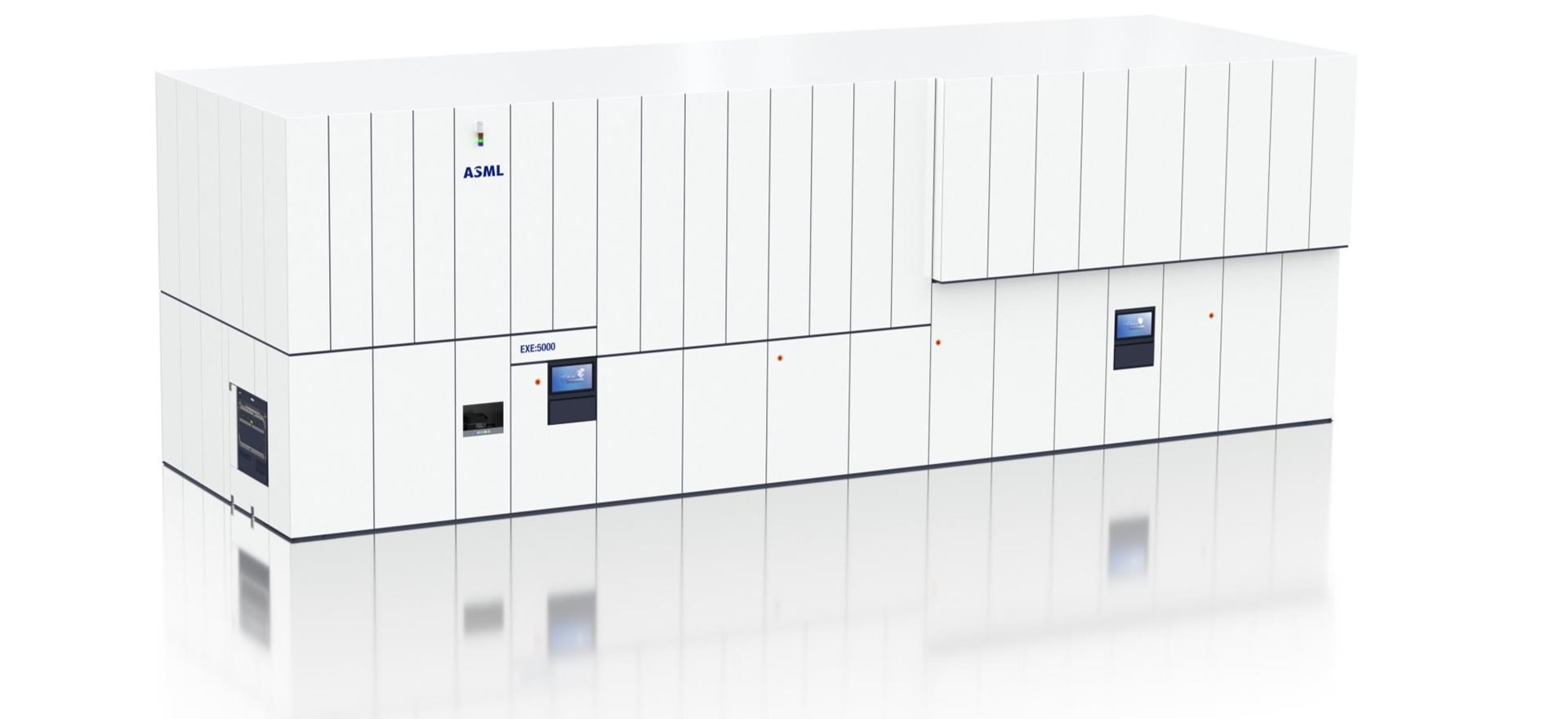
Those three changes are also why Terafab's own target has moved. At the March launch Musk did not repeat the 2nm figure he had used before it, Tom's Hardware noted, and on Tesla's earnings call on 22 April he named a different one: Intel's 14A, a 1.4nm-class process he called "state-of-the-art and in fact not yet totally complete." 14A pairs nanosheets with PowerDirect, and Intel plans it as the industry's first node to use High-NA machines in production, with risk production from 2027 and mass production in 2028. Developing a leading-edge process from scratch can take a decade, by Tom's Hardware's estimate, so the likeliest route is a licence, though Musk has not used the word. There is precedent: GlobalFoundries licensed Samsung's 14nm process a decade ago, and Japan's Rapidus licensed IBM's 2nm. For Intel, whose foundry business lost $10.32 billion in 2025, Terafab would be the first major outside customer for 14A.
The Austin half of the plan is small by comparison, and deliberately so. Tesla broke ground in April on what it calls a research fab on the North Campus of Giga Texas, which Musk described on the April call as a roughly $3 billion project for "maybe a few thousand wafers per month." Its job, he said, is to try out ideas for improving how chips are made, including new physics, and to prove a process works in a production setting before anyone builds it at scale. SpaceX takes the high-volume fab in Grimes County. State construction filings for the Austin work call it simply the "Austin semiconductor fab."
Which leaves the chip. Terafab's website names three: AI5, for Full Self-Driving and the Optimus robot; AI6, for Optimus; and D3, for space. The 2nm chip that exists today is AI5, and Terafab is not making it. Musk announced on 15 April that AI5 had taped out, meaning the design was finished and handed over for manufacture, thanked TSMC and Samsung for their support in production, and predicted it would be one of the highest-volume AI chips in history. The two foundries each make a slightly different version, because, in Musk's words, they translate designs to physical form differently. Samsung's is 2nm: a Samsung Foundry principal engineer wrote on LinkedIn that it would be made "at the Taylor fab using our latest 2nm process", in a post later deleted. The prototype Musk showed carried the marking KR 2613, meaning it was made in Korea in the 13th week of 2026.
Tesla has published almost no specifications. From the module Musk showed, Tom's Hardware identified a compact accelerator die of about half a reticle, surrounded by 12 SK hynix memory packages, which points to a wide memory bus. Performance has not been disclosed beyond Musk's claim of up to 40 times AI4 in certain workloads. Volume is still ahead: Samsung has said it expects volume production of Tesla's AI chips at Taylor in the second half of 2027, and Musk has said Tesla needs several hundred thousand finished AI5 boards before switching vehicle production over. The next chip, AI6, is covered by a $16.5 billion deal with Samsung signed last year.
| AI5 | What is known |
|---|---|
| Designed by | Tesla |
| Made by | Samsung and TSMC, each producing a slightly different version of the same design |
| Process | Samsung's latest 2nm at its Taylor, Texas fab, per a Samsung Foundry engineer. TSMC's process not confirmed |
| Tape-out | Announced by Musk on 15 April 2026; TSMC's version reached it months before Samsung's |
| Die | About half a reticle, the largest area a lithography machine exposes in one shot, by Musk's earlier remarks |
| Memory | 12 SK hynix packages on the module Musk showed |
| Performance | Not published. Musk claims up to 40 times AI4 in certain workloads |
| Volume | Samsung expects volume production of Tesla's AI chips at Taylor in the second half of 2027 |
| Goes into | Full Self-Driving and the Optimus robot, per Terafab's site |
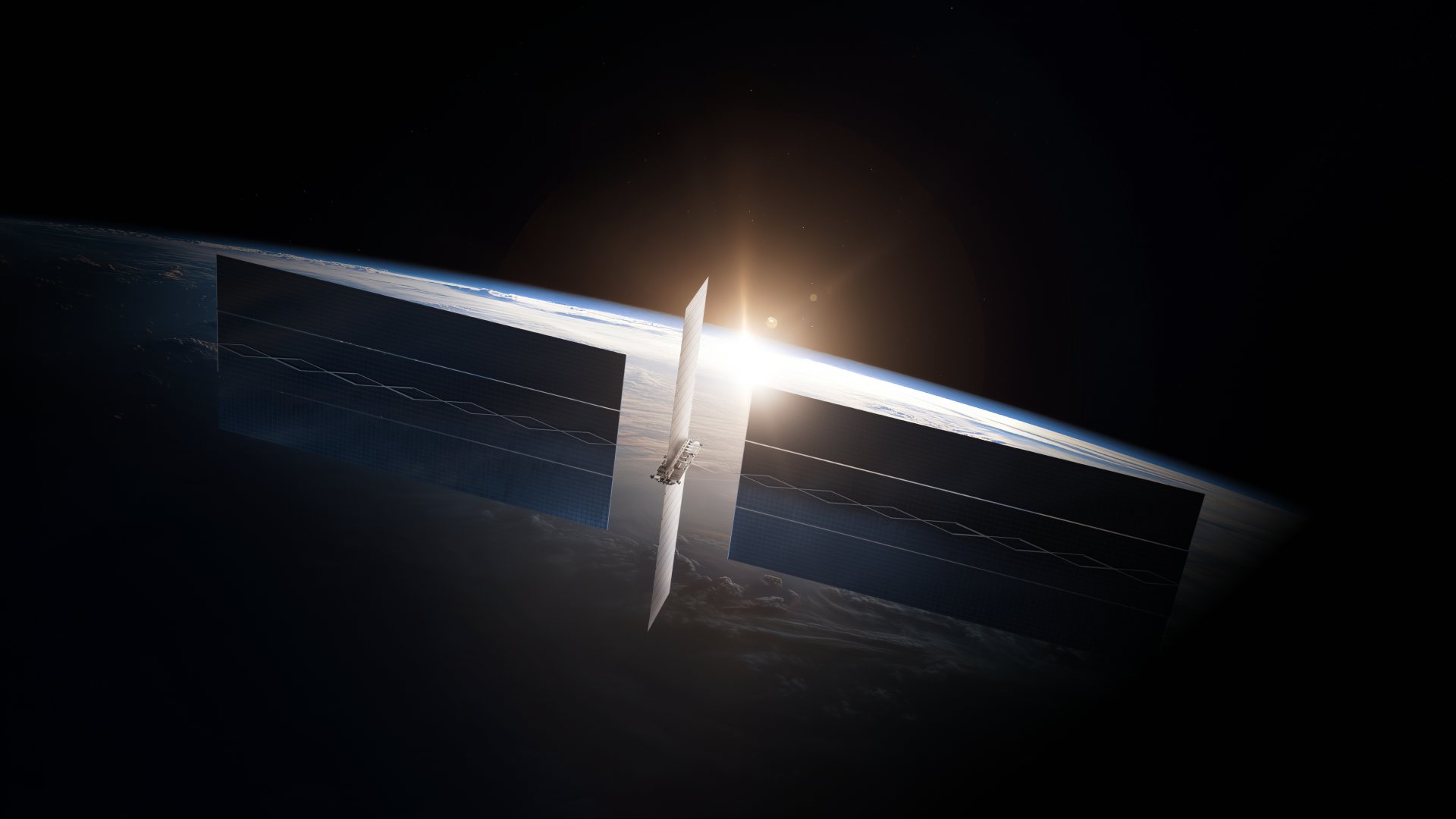
The third chip explains the scale. Musk projected 100 to 200 gigawatts a year of chips for use on Earth and up to a terawatt for space, and said 80 per cent of Terafab's output would go to solar-powered AI satellites. D3 is the chip for those, and he says it will run hotter than terrestrial designs on purpose, because a chip that tolerates more heat needs less radiator to cool it, and every kilogram of radiator has to be launched. SpaceX's own IPO filing is plainer about the risk: nobody has yet operated AI compute in orbit, and hardware that fails there cannot readily be repaired.
The factory will bring its own power plant. Riley Trettel, who leads energy and data-centre development at SpaceX, told a public meeting in August that the company would be "bringing our own power", from natural-gas plants and "very large battery arrays", according to Bloomberg's report as relayed by TechCrunch. Solar has not been mentioned, although Tesla, a partner, sells it. Water, SpaceX says, will come from the reservoir rather than from local groundwater.
Then the fine print. In the amended filing for its stock market listing, SpaceX describes Terafab as a "general framework" agreed with Tesla, with timelines, milestones and capital spending still to be negotiated, warns that it "may not be successful", and notes that neither Tesla nor Intel is obligated to remain part of the project. Bernstein has estimated that the capacity for a terawatt of annual compute would cost $5 trillion to $13 trillion, Reuters reported. And Grimes County, with fewer than 35,000 residents and a tax base of around $11 billion, approved a 100 per cent tax abatement by four votes to one in June, with the county judge saying a negotiated payment in lieu of taxes would bring in $700 million over 35 years.
Two legal fights arrived this month. SpaceX has sued Texas Attorney General Ken Paxton and Grimes County in a Travis County court to stop the release of its tax-abatement application and negotiating records, after the attorney general's office ruled on 28 July that most of them should be released; SpaceX argues disclosure would cause it substantial competitive harm. And Tesla, SpaceX and SpaceXAI have asked a federal court in Austin to declare that the name Terafab does not infringe TERA-FAB, a trademark registered in 2021 by TERA-print, a small Illinois nanotechnology company, for desktop printers that draw microscopic patterns for researchers. No court has ruled on either.
Put together, Terafab is two things at once. The ambition is a single building with, by Electrek's reckoning, more than ten times the floor space of TSMC's biggest fabs, feeding a satellite industry that does not exist yet. The concrete part is smaller and more interesting: a $3 billion research line testing whether one company can loop from mask to tested chip faster than a supply chain spread across several firms, a would-be first outside customer for Intel's first High-NA process, and a construction start listed in state filings for 1 December, with completion by the end of 2028. The 2nm chip that matters to Tesla this year is being made in Taylor, Texas, by Samsung. Whether the generation after it comes out of Terafab is the question the next two years will answer.
| Fact | Detail |
|---|---|
| Launched in | The Seaholm Power Plant, a decommissioned power station in downtown Austin |
| To be built on | The cooling reservoir of a coal plant that ran from 1982 to 2018 |
| Floor space | 100 million square feet, against 10 million for Giga Texas, by Terafab's own figures |
| Chips it names | AI5, AI6 and D3, the last for satellites |
| Output goal | 1 terawatt of compute a year. Terafab's site gives current US consumption as 0.5 terawatts |
| Jobs | 3,000 promised; 10 required by the state incentive agreement |
| Wafers a month | A few thousand at the research fab; 1,000,000 as the long-term goal |
| Tin droplets | 50,000 a second, vaporised by laser in every EUV light source |
| The website | Signed off "Designed and built with Grok", xAI's chatbot |
| The name | TERA-FAB has been a registered trademark since 2021, for desktop lab printers made by an Illinois company |